See Beyond the Surface
Unlocking 3D Metrology with Quantum Sensing
Technology
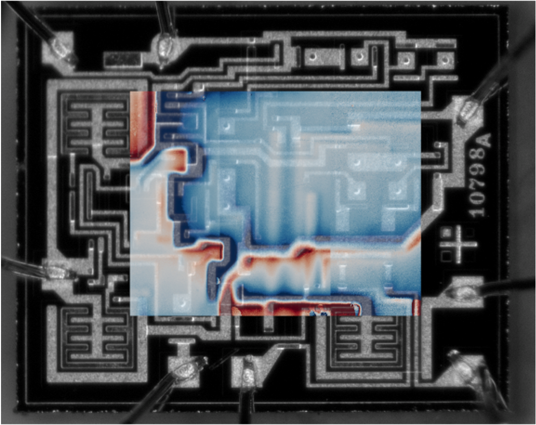
EuQlid's magnetic imaging technology uses quantum defects in diamond to map buried electrical currents.
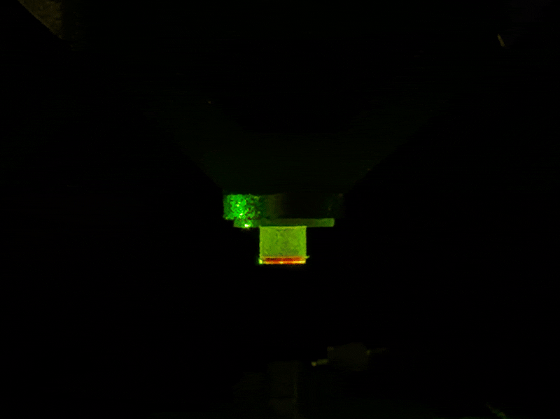
Safely identify defects in complex materials and devices.
Applications
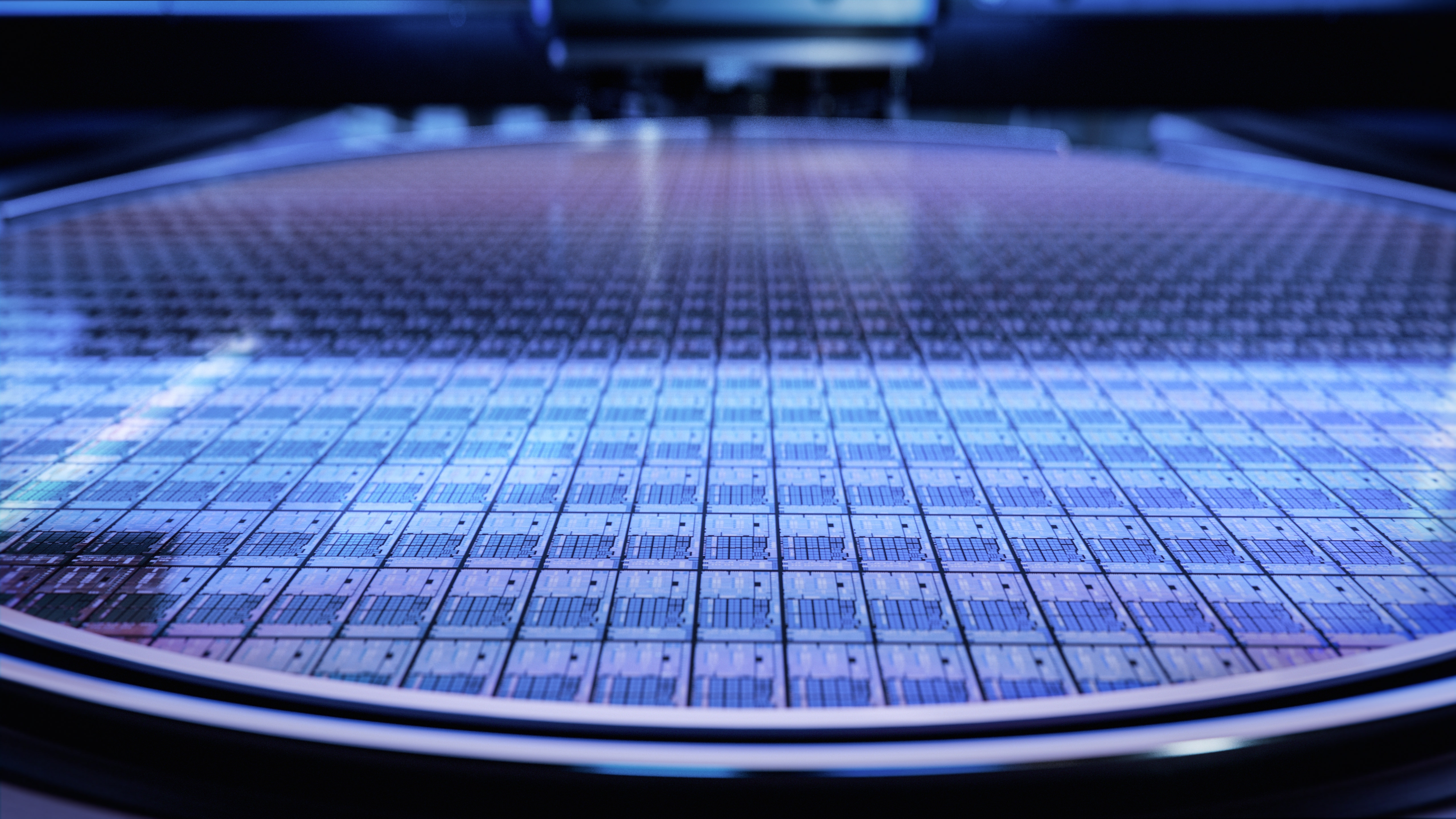
Advanced Packaging
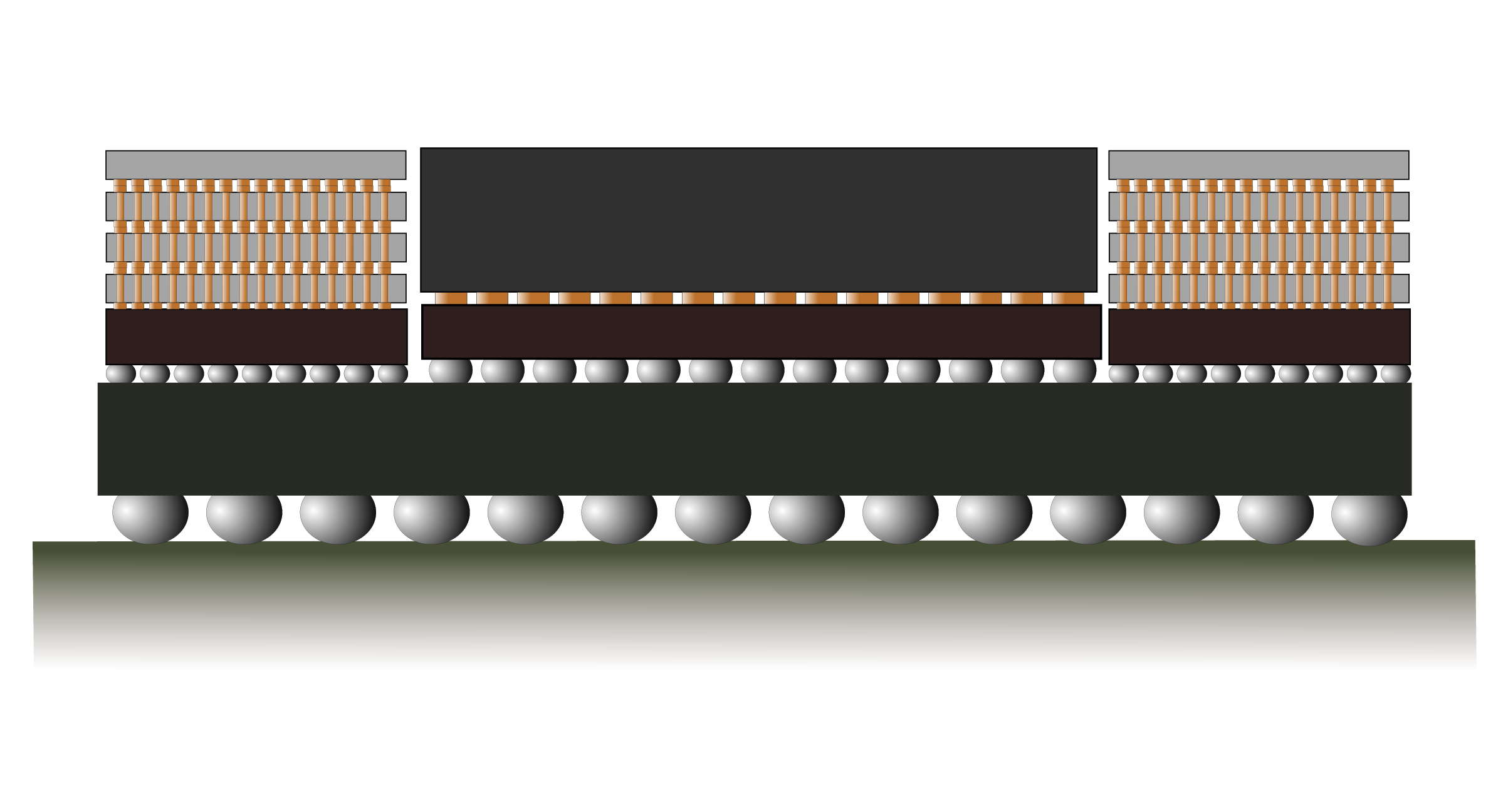
Next-generation semiconductors require 3D architectures to deliver improved performance, cost and power. EuQlid's magnetic imaging solution addresses a foundational need for non-invasive identification of buried connectivity defects during design and high volume manufacturing.
Silicon
Backside Power Delivery and other 3D architecture innovations pose novel challenges for metrology. EuQlid's solution enables spatial analysis of state-dependent power flows in functioning devices to accelerate the validation of new processes and designs.
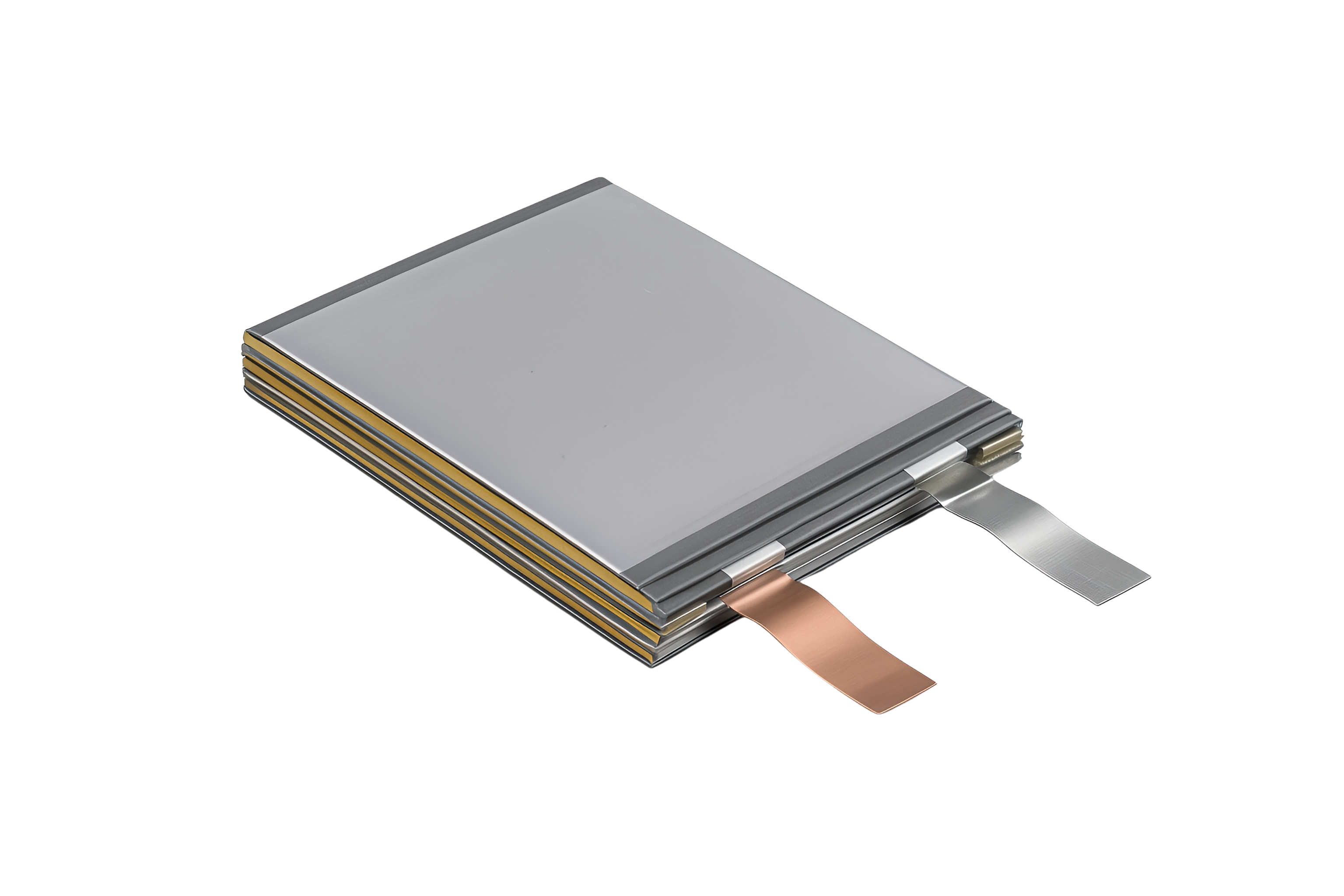
Energy Storage
Improving battery lifetime, safety and performance requires understanding exactly how and where degradation initiates and propagates. Magnetic imaging enables visualization of the spatial and temporal current heterogeneities key to mitigating degradation.
Product
Quantum Diamond Microscope
Magnetic imaging in the lab. Available Now.


Investors